SK Hynix just beat Samsung and TSMC to the punch and made history in the memory chip race, becoming the first company to commercially use ASML’s High-NA EUV technology and future proof the future of DRAM,
Industry Milestone
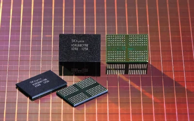
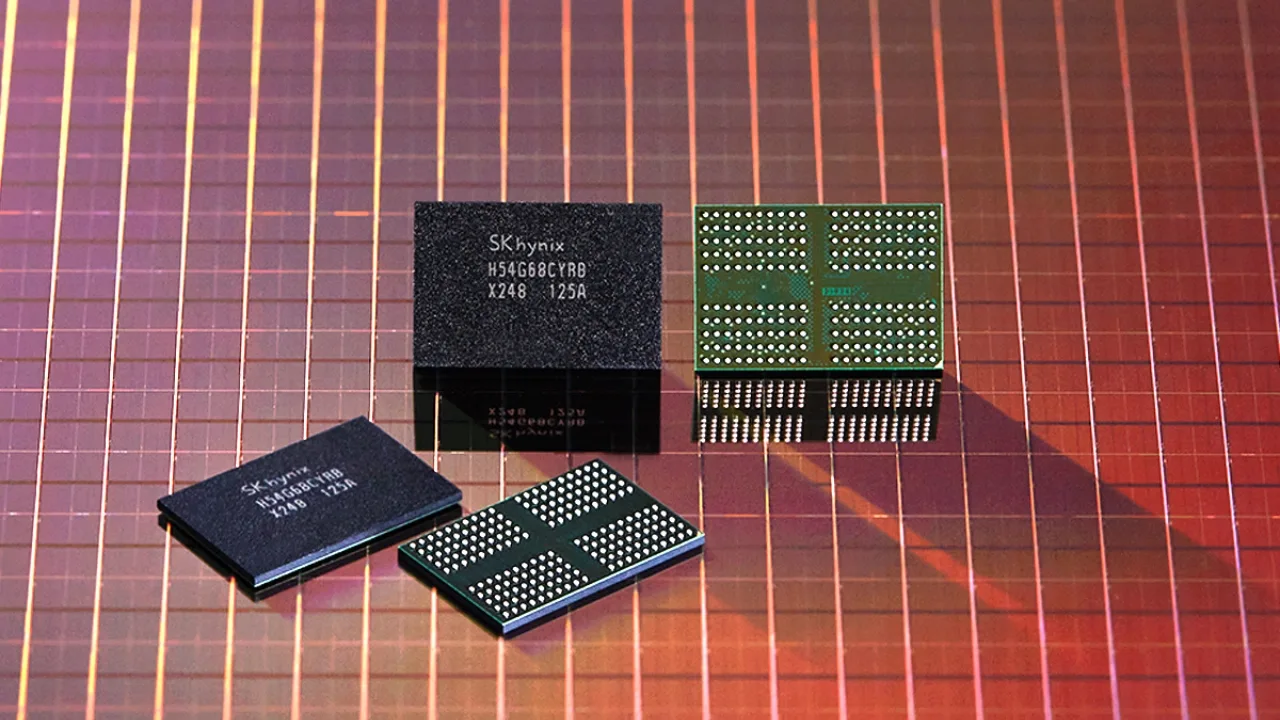
SK Hynix has made history by being the first to add ASML’s High-NA EUV systems into its Icheon, South Korea-based M16 fab, according to a significant announcement. With this move, SK Hynix has become the world’s first company to use the High-NA EUV leaving the likes of Samsung and TSMC behind.
That tool, ASML’s TWINSCAN EXE:5200B, is the High-NA EUV flagship and a whole new generation of litho tool. It allows for smaller transistor sizes (1.7× smaller than current EUV systems) and higher densities (2.9× smaller than current EUV systems) and allows for an increase in numerical aperture (NA) from 0.33 to 0.55 (40% increase).
Why It Matters
High-NA EUV is more than a technical step up. For SK Hynix, it represents:
- Where: A simplification of the EUV process flow.
- Quicker next-gen DRAM development cycles.
- Improvement in product efficacy and economic viability.
- Improved competitiveness in the high-margin memory market.
This accomplishment makes SK Hynix another bang to semiconductor with another boss under the belt, with NVIDIA and AMD as big partners to boast of.
Surpassing Samsung and TSMC
Samsung and TSMC are generally seen as the first and second most important advanced manufacturing firms, but in one key area SK Hynix has unseated its Korean rival: the first commercial High-NA EUV.
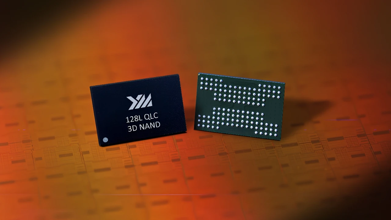
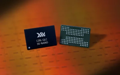
Previously, there had been reports that SK Hynix was developing six EUV layers of DRAM expansion — a goal that was, at best, ambitious. With ASML’s next-gen machinery in place, however, those goals are suddenly achievable.
The Path to Next-Gen DRAM
High-NA EUV will therefore enable DRAM with record high capacity and perform with record high efficiencies, an important development that SK Hynix approaches. This will not only boost the performance of memory but also be a resurgence in cost competitiveness in the market.
This could lead to a semiconductor innovation leap, experts claim, urging Samsung and TSMC to swiftly embrace High-NA technology of their own.
Client Partnerships Driving Growth
SK Hynix is already seen as a high-end DRAM provider, with NVIDIA and AMD ships full of its DRAM solutions. We are now able to confirm that this High-NA EUV breakthrough confirms what we already knew: that the most technologically advanced DRAM here todaymanufacturers are doing it.
What’s Next?
From here, SK Hynix is likely to:
- Scaling production of High-NA EUV tools.
- Add layers of DRAM that go beyond records.
- Fortify its leadership position in next-generation memory technologies
By doing this SK Hynix has indicated that it is not only ahead of Samsung and TSMC but all others in the industry.
FAQ
SK Hynix makes the first adoption of ASML High-NA EUV system that reaches the commercial level to produce the next-gen DRAM.
1.7x smaller transistors, 2.9x higher density, and 40% higher resolution, process simplification, cost down.
As other rivals are still at the planning stage, SK Hynix has already associated ASML’s TWINSCAN EXE:5200B system with production.
SK Hynix advanced DRAM technologies and high end are expected beneficiaries to major clients like NVIDIA, and AMD.
Expand DRAM stacking, enhance competitiveness, and accelerate the advanced memory leader.