Test post title
Test post content

Test post content
Test post content
Test post content
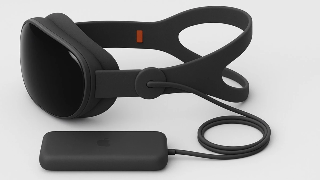
Everything Apple ProApple Vision Air: Why a lighter design, iPhone A-series chip, and starting at $1,750 could make Apple mixed reality more affordableSobler style)Apple Vision ProApple Vision ProApple Vision ProApple Vision Pro Will 2027 be the The Year Apple’s Mixed Reality Headset Goes Mainstream? Apple Vision Air could be the device that drives spatial computing … Read more
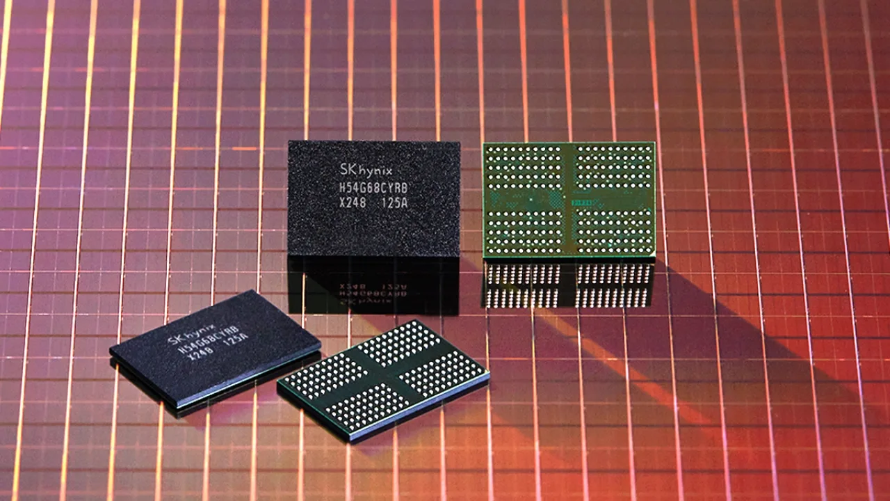
SK Hynix just beat Samsung and TSMC to the punch and made history in the memory chip race, becoming the first company to commercially use ASML’s High-NA EUV technology and future proof the future of DRAM, Industry Milestone SK Hynix has made history by being the first to add ASML’s High-NA EUV systems into its … Read more
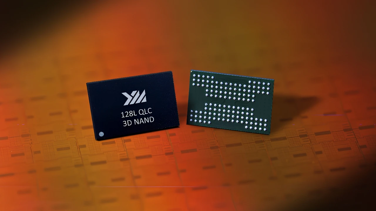
In tandem with a prelude of entry and competition in DRAM between the NAND flash giant, YMTC, and China’s top tier in DRAM field, CXMT, plans for YMTC DRAM HBM have come to the surface. According to reports, the partnership between YMTC in DRAM HBM is for hybrid bonding and HBM technologies, which cover not … Read more
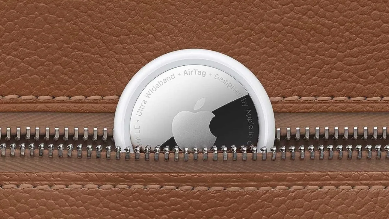
For a traveler, losing baggage at the airport is actually a nightmare. However, one passenger at Los Angeles International Airport (LAX) was able to turn a panic into a feelgood technology-good story, using Apple‘s AirTag to track down his lost bag once it was missing. Last month, a suitcase hidden inside an AirTag was able … Read more

What do you get if you mix morality, survival and freedom of narrative in a vampire RPG? Back in 2025 at Gamescom, Rebel Wolves announced The Blood of Dawnwalker, a sandbox RPG where every decision — from whether you feed on humans or embrace your vampirism — affects protagonist Coen’s journey. From its plague-ridden setting, … Read more

The AMD Magnus APU will cost Xbox Next almost twice as much as PlayStation 6, plus with Microsoft opening the door for third-party stores, the console war now has a new changing factor. The console war is heating up, and this time, Xbox Next may not just be news for its power — but for … Read more
Cambricon stock mania, the hottest topic of the Chinese AI chip sector. The stock’s meteoric ascent has earned it Wall Street attention that Goldman Sachs is doubling down on bullishly. But behind the euphoria, there are serious risks. Once shunned as the “king of losses,” Cambricon Technologies, or Hanwuji as the company is locally known, … Read more
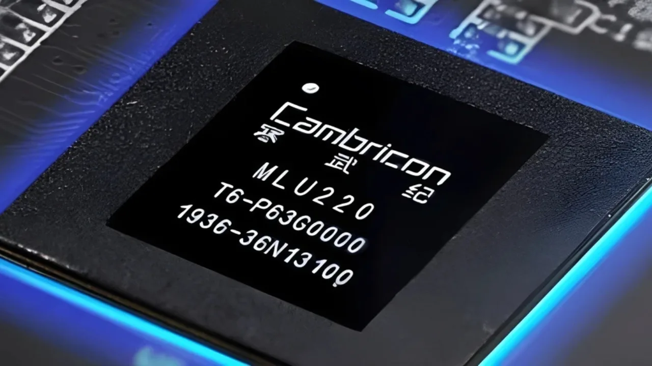
Cambricon‘s stock is on fire, and the company’s soon to become the hottest creature in China’s artificial intelligence (AI) chipset sector. The company’s stock has soared — and caught the attention of Wall Street — prompting Goldman Sachs to double down on its bullish outlook. But beneath the euphoria, serious perils remain. Once derided as … Read more
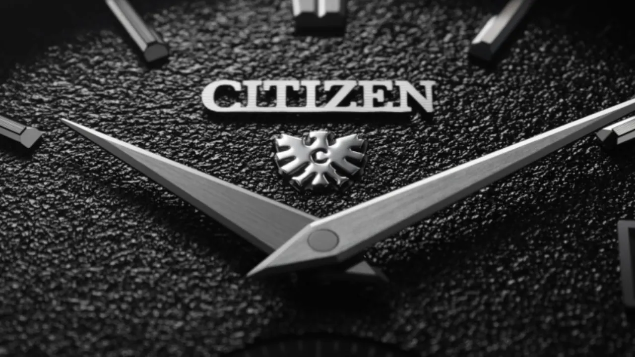
From October 2025, the global watch warranty will fleece Trusted Reviews for Citizen’s 3 years. Now, a major update brings all coverage in all regions under one standard. If you have ever purchased a Citizen watch, then you already know about the brand name the durability and new technology. Recently, Citizen took a bold step … Read more